



Transparent Electronics
Advanced nanometric formulations for transparent, conductive surfaces.
Invisible conductivity. Unseen performance.
A subsidiary of GenesInk Group, GNKVIEW develops highly transparent, conductive nano-solutions tailored for the transparent electronics sector.
At the crossroads of photonics, material chemistry, and advanced user interfaces, GNKVIEW provides an industrial alternative to ITO, redefining the possibilities for smart glass.
Smart Glasses & Windows, Transparent Photovoltaics, Transparent Heating & Defrosting, Transparent Sensors & Surfaces
Our transparent conductive films (TCF) and grid formulations meet the specific requirements of printed optoelectronics, combining exceptionally low haze, high transmission, and industrial reproducibility compatible with complex substrates.
When conventional solutions reach their limits,
GNKVIEW unlocks the potential of transparent surfaces.
Key Markets
Smart Glasses & Windows, Transparent Photovoltaics, Transparent Heating & Defrosting, Transparent Sensors & Surfaces.
Challenges
Optical transparency, flexible and curved surfaces, high resolution, miniaturization, device lightweighting, surface functionalization.
What GNKVIEW Unlocks
Connected glass and windows, transparent heating, transparent sensors and antennas.
Technologies: Transparent Electrodes · Transparent Conductive Films (TCF).
GNKVIEW supports manufacturers, OEMs, laboratories and integrators, from formulation customization to industrial scale-up.
Explore our applicationsKey Performances
// Invisible ConnectivityTransparency
// 01Optimal optical clarity.
Sheet resistance
// 02High performance, flexible connected.
Flexibility
// 03Low friability.
Patterning
// 04Low friability. Seamless integration. Material use optimisation.
Visual Connectivity
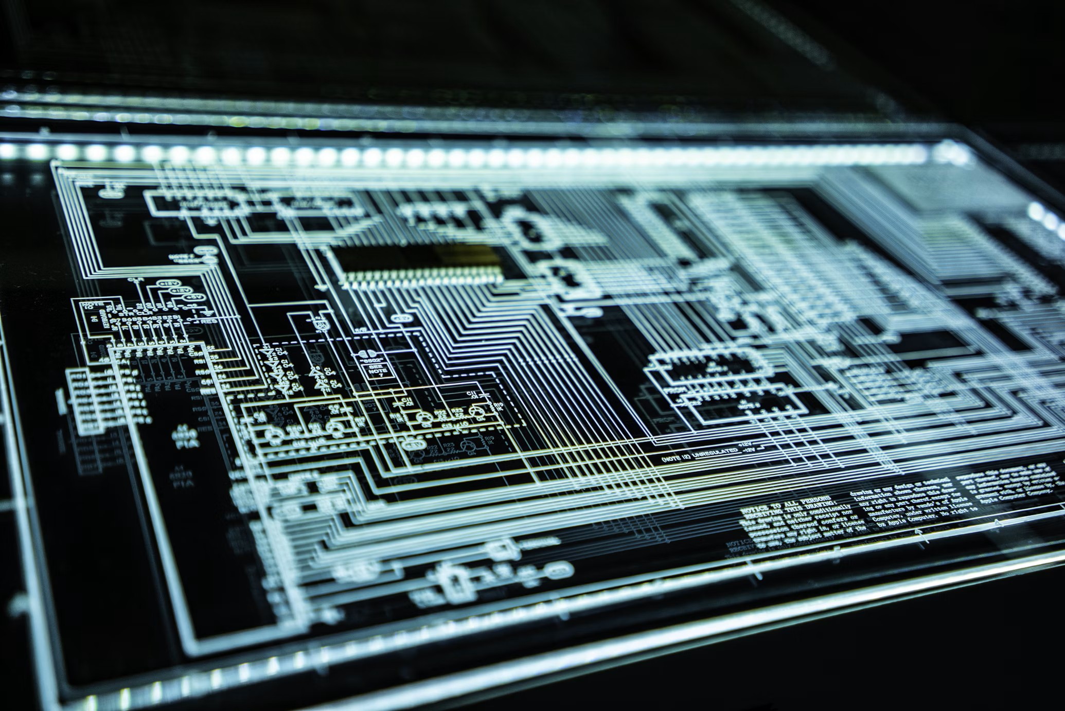
High conductivity combined with optimal optical transparency. We push the boundaries to make circuits invisible to the eye while maintaining superior electrical performance.
- High Transmission
- Low Resistance

Mechanical Flexibility
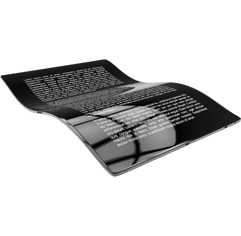
Suited for soft and curved substrates. As displays move beyond flat screens to wearable and foldable devices, our inks flex without cracking.
- Wearables
- Curved Surfaces
Seamless Integration
Additive patterning for seamless connectivity and natural integration into advanced display architectures. We simplify the stack by reducing layers.
- Simplified Stack
- Additive Process
Offer
// From R&D to Licensing
Prototyping
Pattern optimization and prototyping on target substrates.
Formulation Co-development
Adaptation to support performance objectives.
Process Engineering
Seamless integration into existing manufacturing lines.
Operating Licenses
Technology transfer for autonomous operation.
// CORE Offer
Formulation Co-development
Proven formulations. Expertise to evolve them.
Our formulation portfolio is a scalable technology foundation for your developments.
Accelerate your time to market
Mature, industrializable formulations designed to reduce your qualification phases.
Easily integrate our formulations into your processes
Broad compatibility with all industrial printing processes and a wide range of substrates, including flexible and heat-sensitive ones.
Create products your competitors cannot design
We select the formulation best suited to your application, then customize it when your project demands unprecedented performance.
Prototyping
From idea to functional display device — faster, smarter, with the right technologies.
Our ambition is to drastically reduce the time between the initial idea and the first operational prototype. GNKVIEW supports display manufacturers throughout their design and prototyping phases.
Intelligent Optics Design Platform
Specifically developed to balance optical transmission and electrical conductivity in complex transparent architectures from the earliest design stages.
- Simulate Haze vs. Sheet Resistance
- Optimize grid invisibility
- Secure designs & control costs
Expert Support & Co-Design
Our experts provide tailored design support, drawing on their in-depth mastery of Silver Nanowires (AgNW). We help you define relevant architectures and secure technical choices pre-prototyping.
Rapid Prototyping
A dedicated clean-room printing facility enabling a fast transition from design to physical device. Hybrid approach suited for innovation phases and proof-of-concept.
Product Families
// Our Technologies
High Performance Conductive Inks
Key Uses
High-performance electrical conductivity, micron-scale printing resolution, electrical continuity on fine lines, performance-to-material-cost optimization.
Key Functionalities
Charge transport control, Layer uniformity & crystallization
Transparent Conductive Inks
Key Uses
Fine transparent lines & circuits, Transparent flexible electrodes & ITO replacement layers for photovoltaics
Key Functionalities
High transmittance, High optoelectronic FoM, Haze control, Mechanical flexibility
Semiconductive Inks
Key Uses
Functional layers (ETL, HTL, top electrode), organic & perovskite active layers
Key Functionalities
Charge transport control, Layer uniformity & crystallization
// Universal Compatibility
Methods
Substrates
// Transparent Electronics
Transparent Conductive Inks
Silver-nanowire transparent conductive inks for flexible transparent electrodes. High transmittance and low sheet resistance. Filter by printing process and request the technical data sheet.
| Printing process | Sheet resistance (mΩ/□) | Light transmittance (%) | Technical Data Sheet | Reference |
|---|
Request the Technical Data Sheet

// In the Press
Scientific Publications
Selected news, publications and breakthroughs around our transparent electronics inks.
Process Engineering
Optimize coating processes and ensure optical reproducibility.
GNKVIEW supports industrial partners and system integrators in the operational deployment of our transparent solutions within their production lines. Our approach ensures optimal and compliant use of our technologies, taking into account your specific coating equipment.
Identification
Of technical challenges and process bottlenecks before integration.
Control
Ensuring fully controlled and reproducible coating processes.
Performance
Achieving transparency and resistance levels aligned with expectations.
Efficiency
Optimized setup and parameterization time for faster production.
Operating Licenses
Technology transfer for autonomous use of our expertise within a defined geographical or industrial scope.
Ready for Transparency?
Design next-gen interfaces with our transparent conductive inks.