The 100 Patents and Tech Awards of the French Tech Inventors reveals the 100 most inventive start-ups. This ranking also reveals five main lessons.
GenesInk ranked 21st position out of the 100 selected start-ups!
We are proud that our investments in R&D are to be recognized and we strive to bring our customers the best and most easy to use electronics inks on the market.
The first proofs of concept allowing the realization of subsystems manufactured by printing have just been realized with a second generation transistor technology. This step paves the way for the development of application demonstrators with optimized electronic integration.
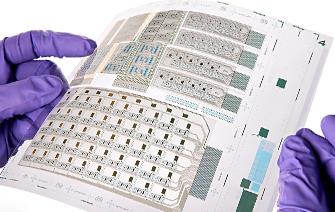
Developed for more than 10 years at the Liten, an institute of CEA Tech, printed electronics on flexible organic media has taken an important step forward in the European ATLASS project. While proof of concept had already been done on the scale of components and simple circuits, the printing of transistors on plastic substrates had not yet been demonstrated on a pilot line with sufficient performance and efficiency levels for the manufacture of complex circuits and subsystems. It is now done!
Working closely with ink and printing equipment suppliers, Liten has optimized the materials and printing process (including engraving of printing rollers) to achieve the efficiencies required to scale up. The process reliability has also been improved to achieve a near-zero defect rate and perfect reproducibility of the components. Several samples of a few hundred to a few thousand transistors were produced with 0 defects (100% functional components). This optimization and maturation work has enabled the prototyping and realization of functional demonstrators based on printed transistor circuits in the field of the Internet of Things and Intelligent Sensor Surfaces. The interest of the technology will now be tested for various applications.
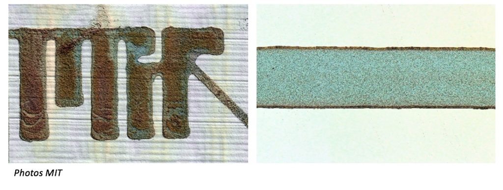
MIT researchers have developed a simple, low-cost method to 3-D print ultrathin films with high-performing “piezoelectric” properties, which could be used for components in flexible electronics or highly sensitive biosensors.
High-frequency devices are key enablers of state-of-the-art electronics used in a wide and diverse range of exciting applications such as inertial navigation, communications, power conversion, medicine, and parallel computing. However, high-frequency additively manufactured piezoelectric devices are yet to be demonstrated due to shortcomings in the properties of the printed transducing material and the attainable film thickness. In this study, we report the first room-temperature-printed, piezoelectric.
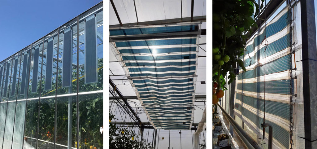
Within the framework of a partnership with Eiffage Energie Systèmes, Les Maraichers Nantais and Groupe Olivier, ASCA® photovoltaic films have been deployed at industrial greenhouses located near Nantes. Covering 43m² and incorporated in three different ways, the project aims to demonstrate the merits of the ASCA® organic photovoltaic film and its ability to meet the specific needs of producers.
With this demonstration, the producers and Eiffage Energie Systèmes are seeking to measure the contribution of organic photovoltaic film as both a low-carbon energy solution and as a regulator of luminosity and thermal conditions.
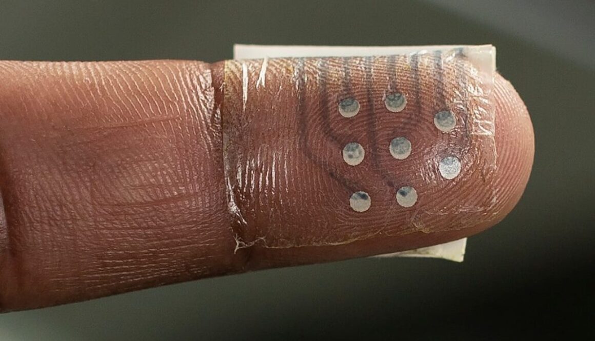
Stanford engineers have developed a way to detect physiological signals emanating from the skin with sensors that stick like band-aids and beam wireless readings to a receiver clipped onto clothing.
Their goal was to create a technology that is comfortable and easy to use with no batteries or rigid circuits. The design was eventually successful with variations of the RFID technology. The similar technology used in an ID card, when the person holds up the ID card to a RFID receiver, an antenna in the ID card returns RFID energy from the receiver and uses to produce a code and guides it back to the receiver. The BodyNet sticker works in a similar manner to that of an ID card. It also has an antenna that yields the inward RFID energy from the receiver on the clothing to the power its sensors. The readings are then transferred from the skin and send them back to the receiver.
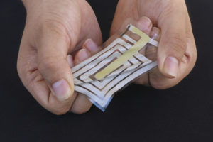
Using metallic ink, researchers screen-print an antenna and sensor onto a stretchable sticker designed to adhere to skin and track pulse and other health indicators, and beam these readings to a receiver on a person’s clothing.
The development of IoT, sensors and smaller electronic devices pushes printed electronic manufacturing towards its limit. Form factor reduction is a must, and screen-printed electronics require now finer printed lines as well as thinner substrates.
When targeting fine lines, current products show their limits: strong resistivity, poor homogeneity, step effect for multilayer printing.
When looking to decrease the device thickness, substrate choice is a key parameter. Reduction of substrate thickness below 50µm, down to thickness such as 25µm, allows new applications. It is today limited by substrate surface waves resulting from adhesion during curing, but also by material thickness and dielectric passes.
GenesInk team will expose the possibilities for fine line printing as well as ultra-thin substrate electronics thru examples and existing technical solutions available at mass production scale.
Schedule (click on selected date and time to register):
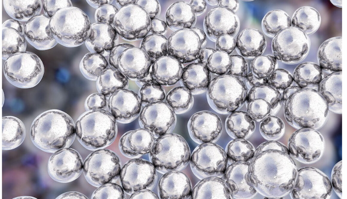
An unexpected ability of cells to bend metal determines the safety of silver nanowires — highly conductive nanomaterials a thousand times thinner than a human hair that are being used in next-generation touchscreens for smartphones and consumer electronics, a transnational team of scientists that includes University of Florida researchers has found.
GenesInk TranDuctive® inks based on silver nanowires are ready for production and next generation touchscreens!
As the appetite grows for devices based on transparent conductive film, cheaper and more flexible formulations have to be found. CLEARSILVER pioneered a nanosilver and nano zinc-oxide printing process suited to organic photovoltaic and organic light-emitting diode applications.
CLEARSILVER SME Instrument H2020 project – coordinated by GenesInk has ended with success on February 2019. CLEARSILVER pioneered a nanosilver and nano zinc-oxide printing process suited to organic photovoltaic and organic light-emitting diode applications.
Dr Anusha Withana from Sydney University has developed an « electronic skin », meaning a super-thin, hyper-flexible sticky tape that can have electronic circuits printed onto it. Once applied, people could use it to control devices, receive information and importantly, register sensations through mobile phone-like vibrations.
This opens doors to many applications : someone with a robotic hand will be able to sense heat from a cup, or gauge how much pressure to apply to an object. A stroke patient might have a personalized interface with sensors that measure their progress and give them feedback. A surgeon doing surgery remotely could get the same sense of pressure or dexterity that they would have if they were there in person.
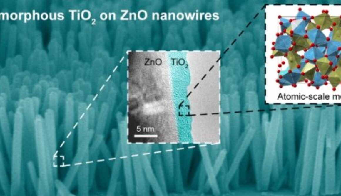
Scientists from the Center for Functional Nanomaterials (CFN) – a U.S. Department of Energy (DOE) Office – have come up with a technique for optimizing the activity 500-nanometer-long but relatively thin (40 to 50 nanometers) nanowires, made of zinc oxide (ZnO).
Those nano wires could be used as catalyst for triggering surface electrochemical reactions to generate clean and sustainable fuels such as hydrogen.
Pour offrir les meilleures expériences, nous utilisons des technologies telles que les cookies pour stocker et/ou accéder aux informations des appareils. Le fait de consentir à ces technologies nous permettra de traiter des données telles que le comportement de navigation ou les ID uniques sur ce site. Le fait de ne pas consentir ou de retirer son consentement peut avoir un effet négatif sur certaines caractéristiques et fonctions.
Fonctionnel
Toujours activé
L’accès ou le stockage technique est strictement nécessaire dans la finalité d’intérêt légitime de permettre l’utilisation d’un service spécifique explicitement demandé par l’abonné ou l’utilisateur, ou dans le seul but d’effectuer la transmission d’une communication sur un réseau de communications électroniques.
Préférences
L’accès ou le stockage technique est nécessaire dans la finalité d’intérêt légitime de stocker des préférences qui ne sont pas demandées par l’abonné ou l’internaute.
Statistiques
Le stockage ou l’accès technique qui est utilisé exclusivement à des fins statistiques.Le stockage ou l’accès technique qui est utilisé exclusivement dans des finalités statistiques anonymes. En l’absence d’une assignation à comparaître, d’une conformité volontaire de la part de votre fournisseur d’accès à internet ou d’enregistrements supplémentaires provenant d’une tierce partie, les informations stockées ou extraites à cette seule fin ne peuvent généralement pas être utilisées pour vous identifier.
Marketing
L’accès ou le stockage technique est nécessaire pour créer des profils d’internautes afin d’envoyer des publicités, ou pour suivre l’utilisateur sur un site web ou sur plusieurs sites web ayant des finalités marketing similaires.