HeliosInk

Image module

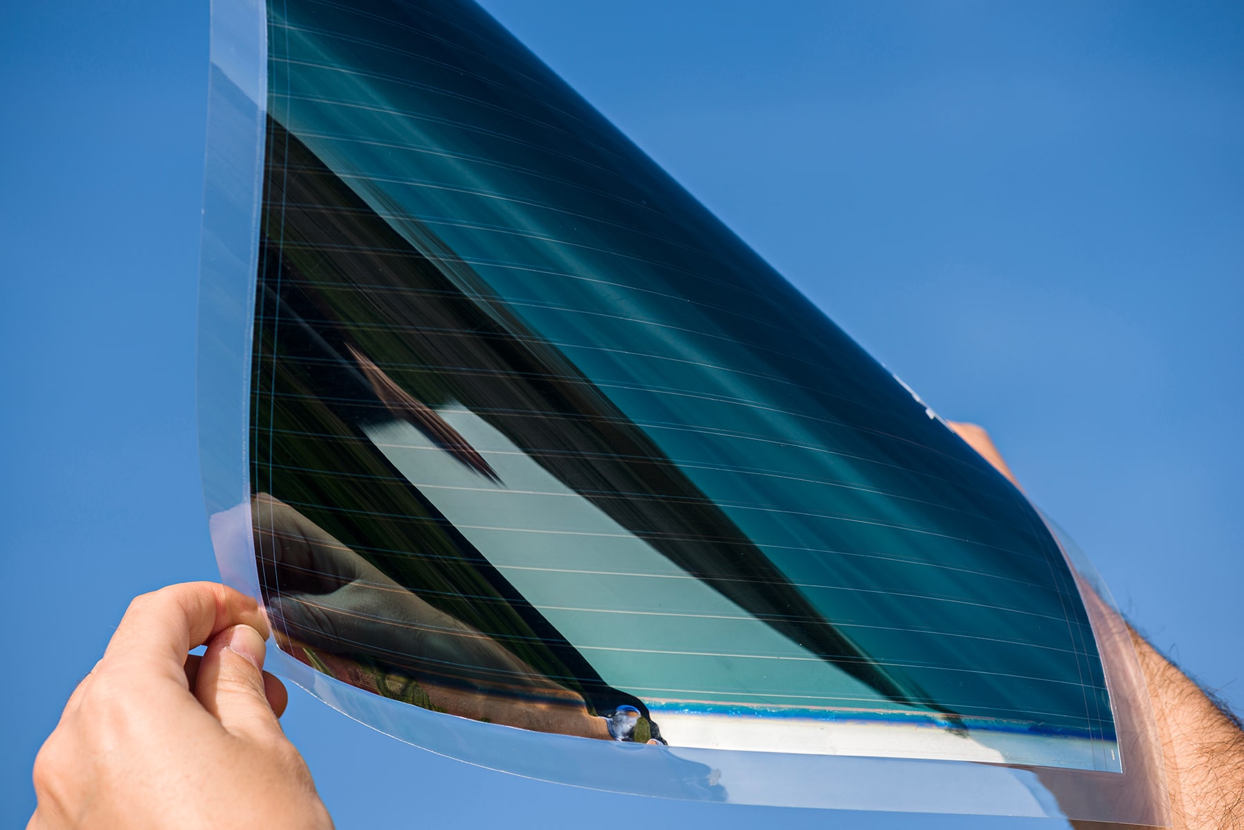
The right choice of semi conductive ink for a more efficient and longer-life OPV device

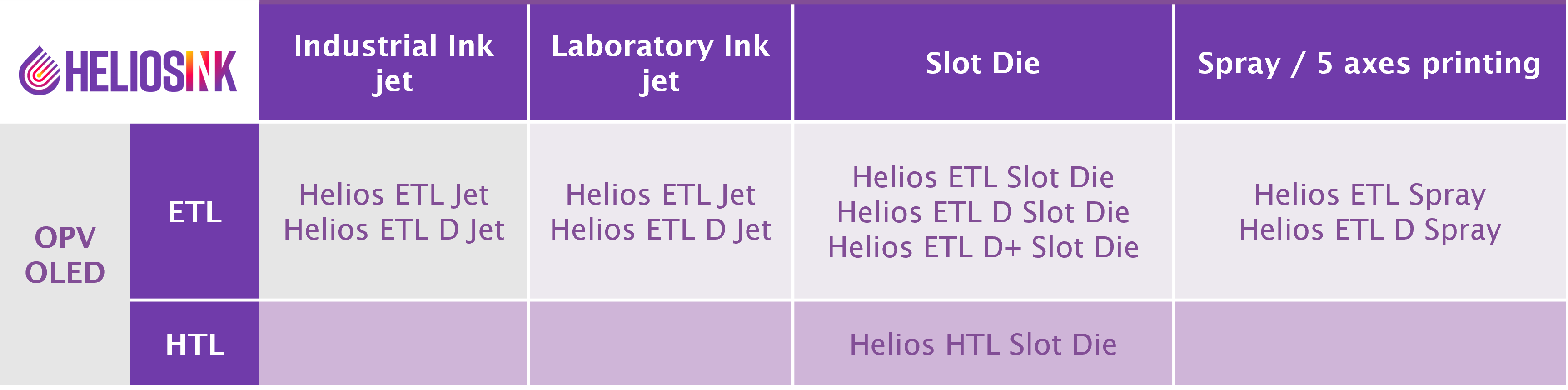
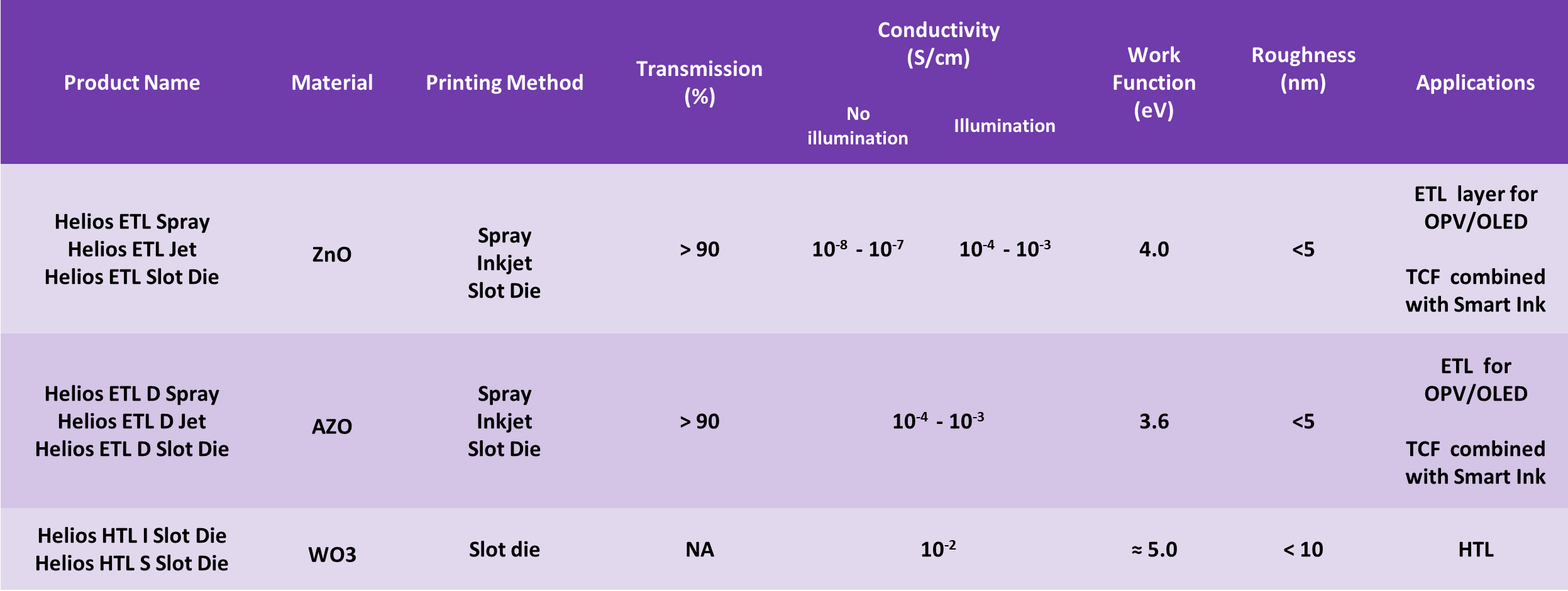
GenesInk’s patented HeliosInk solutions can be used for electrode manufacturing or charge transport layer deposition in OPV cells.

Functions :
> Charge Transport Layers

Image module

Key benefits :

  • Printing on various flexible plastic substrates (PET, PEN, KAPTON, Glass, Polycarbonate, Paper, ITO, Ag NWs layer, Active layer)
  • Improved cell efficiency
  • High transparency (>90%)
  • Protection against oxidation (∆PCE<10% after 2 000h)
  • Protection against aging due to UV exposure
  • Smoother surface

Solutions for brighter and flexible OLEDs.

GenesInk’s patented HeliosInk solutions can be used for electrodes manufacturing or charge transport layer deposition in OLED displays:

Functions :
> Charge Transport Layers

Key benefits :

  • Low curing temperatures for printing on flexible substrates (from room temperature up to 150°C)
  • Compatible with various curing process (IR, Photonic, Industrial Oven, Conveyor Oven)
  • Printing on many different flexible plastic substrates (PET, PEN, KAPTON, Glass, Polycarbonate, Paper, Glass ITO, Ag NWs layer, Active layer)
  • Non-toxic inks / non-CMR solvent
  • Smoother surface

HeliosInk products overview, find the right ink for your application and printing process :

Image module

HeliosInk Product Characteristics :

Image module